
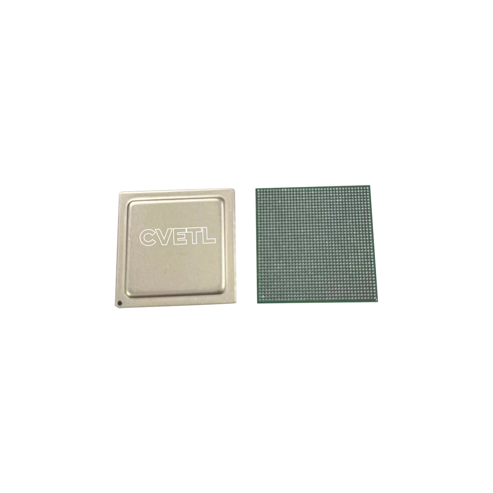
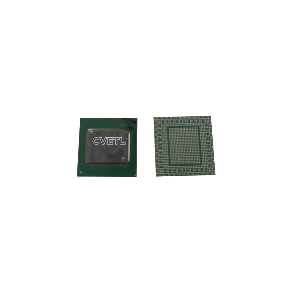
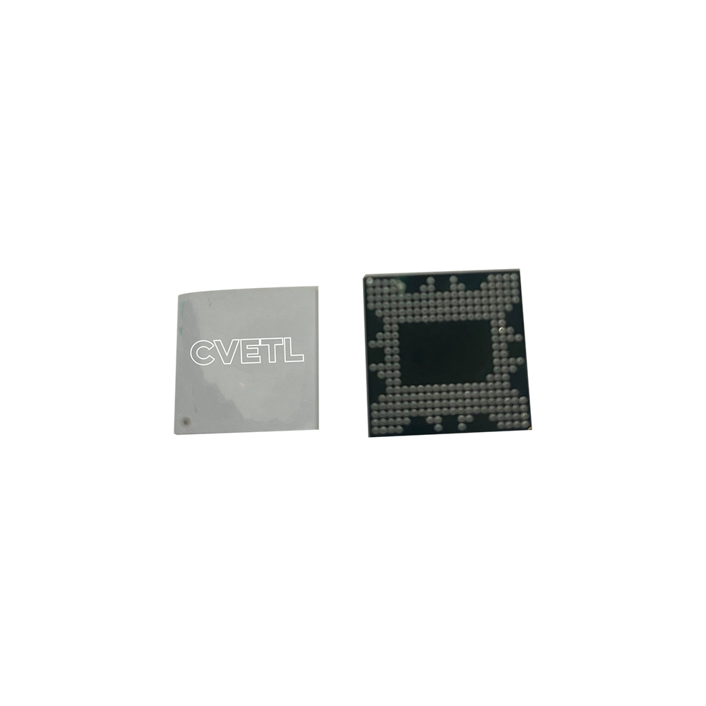
FCBGA
CVETL is now offering Flip Chip BGA package; a flip chip solution for high performance BGA packaging. Area array flip chip bump design utilizes the die area and provides the shortest interconnection path as a replacement for conventional wire bonding. Proprietary assembly process has been developed for this novel packaging. A fine line/space BT base laminate substrate or a blind/buried via, laser drilled build-up organic substrate can be used for Siliconware's Flip Chip BGA packages. Optional heat spreader attaching process can provide a superior heat dissipation of flip chip die, which is suitable for high-end applications.
FEATURES
• 4-8 layers build up substrate
• Optional one piece heat spreader for high thermal requirement
• Minimum 200 µm bump pitch
• Die size up to 30 mm
• Package sizes from 27x27 mm to 45x45 mm
• JEDEC MS-034 compliant, 1.27/1.00 mm pitch BGA footprint
• Package up to 1800 balls