
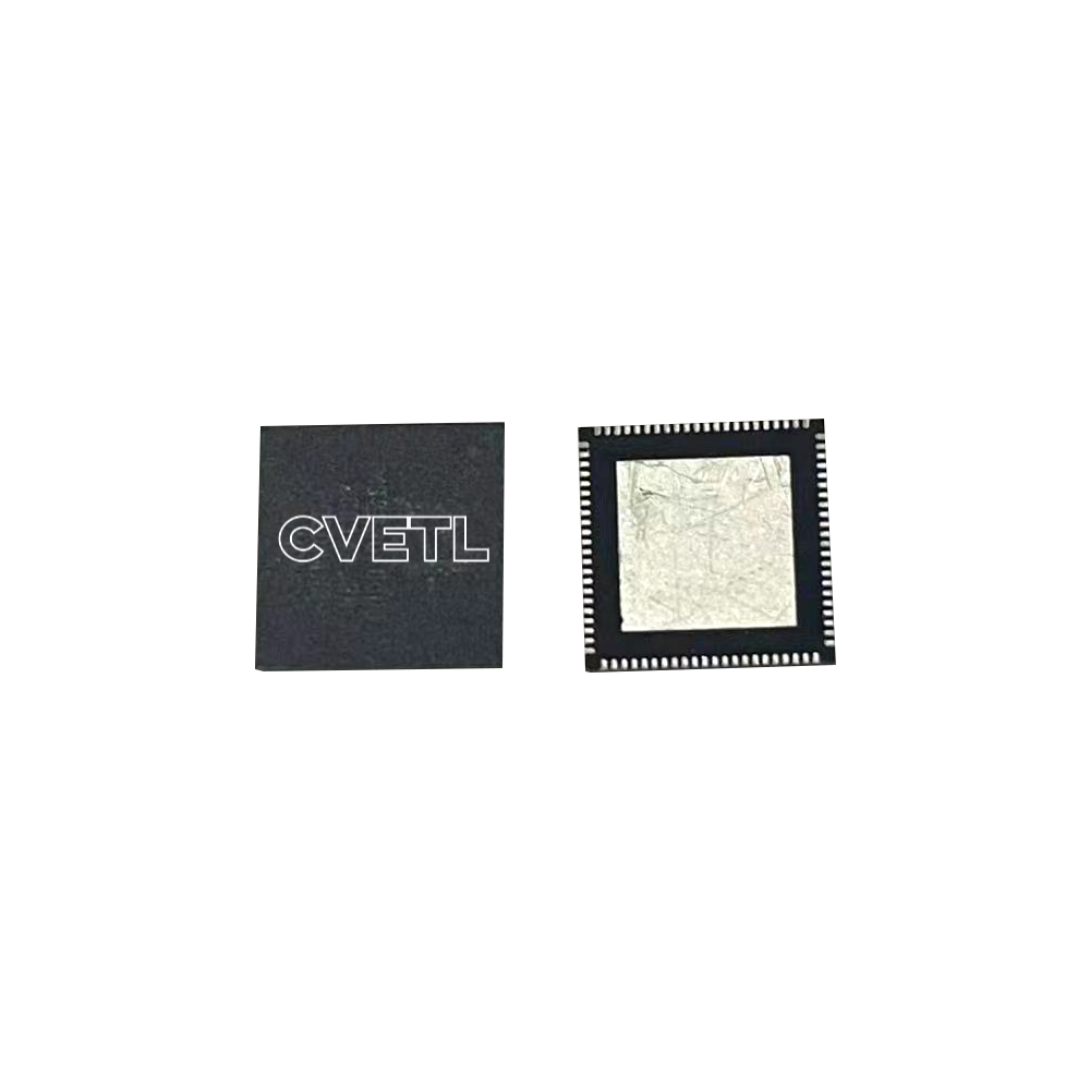
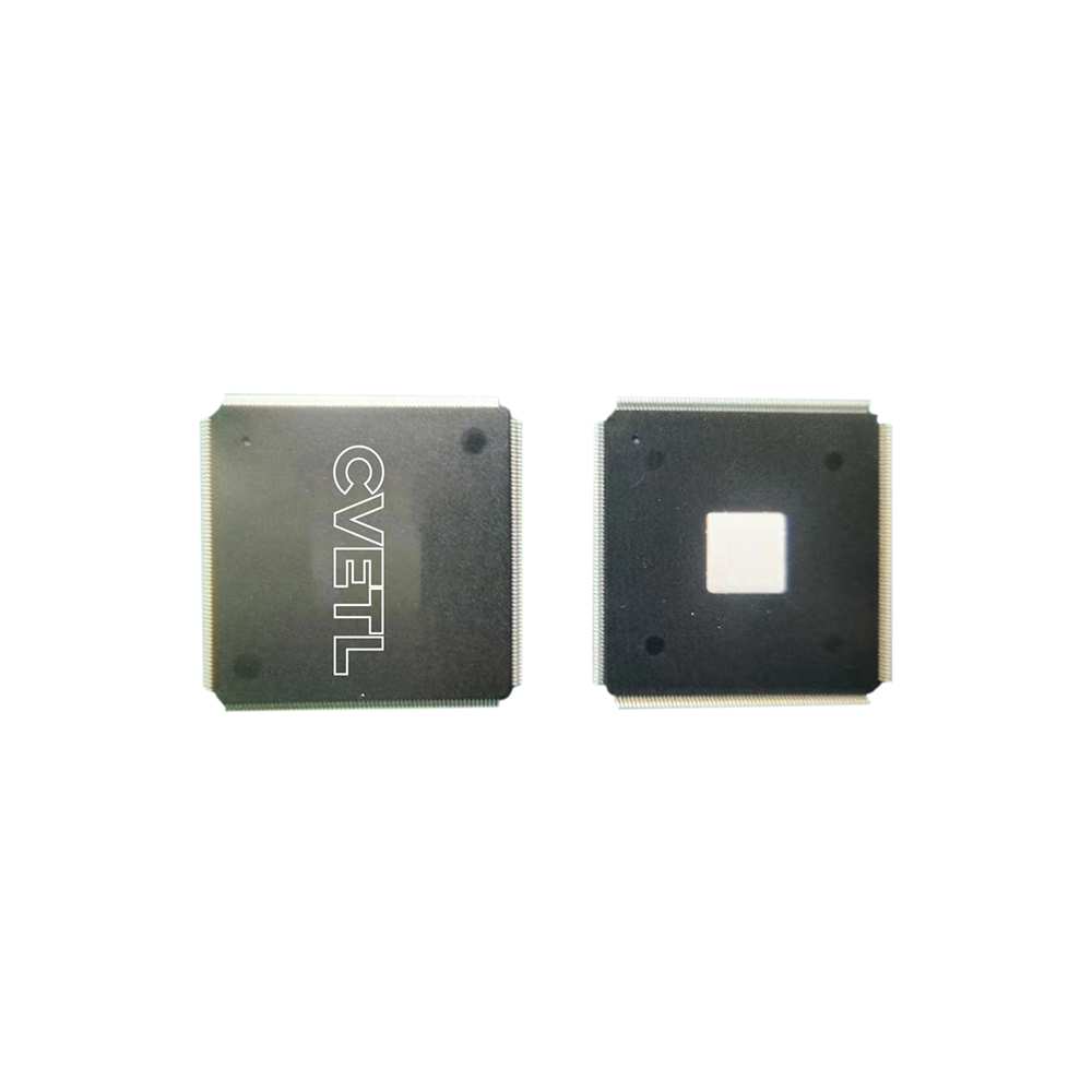
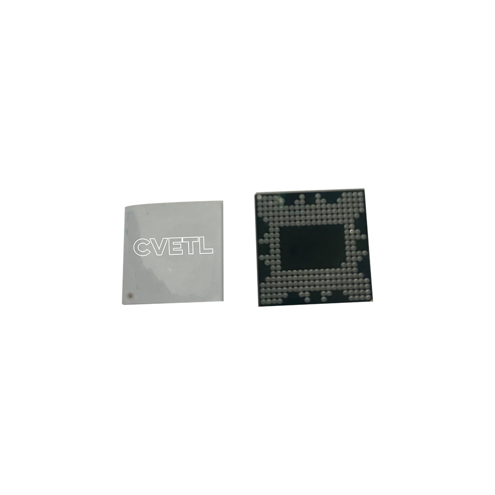
QFN
Cvetl's Quad Flat No-lead, QFN package is a plastic encapsulated leadframe based CSP with lead pad on the bottom of the package to provide electrical interconnection with the printed circuit board. This package offers small form factor with 60% size reduction compared with conventional QFP package. It provides good electrical performance due to the short electrical path in the inner leads and wires. The package also provides excellent thermal performance by an optional exposed die pad to provide efficient heat path soldered on the PCB.
Cvetl now is offering two types of QFN,Punched QFN and Mapped QFN. Mapped one has shorter lead time on development caused by manufacture flexibility for different package size utilizing sawing technology
APPLICATIONS
The small and light package with improved thermal and electrical performance makes QFN suitable for portable communication / consumer products. Applications include cellular phones, PDAs, wireless transmitters, RF front end, HD devices, microcontrollers, pre-amplifiers, servers, smart power suppliers, switches, DSPs, ASICs and wrist watches
FEATURES
• Low profile: ≤1.0 mm
• Small form factor
• (60% size reduction compared with QFP)
• Cost effective leadframe based CSP
• Improved thermal and electrical performance CSP
• Pb-free lead finish available
• 3x3 to 12x12 mm body sizes
• 4 to 104 lead counts
• Full in-house design ability
• JEDEC standard outlines