
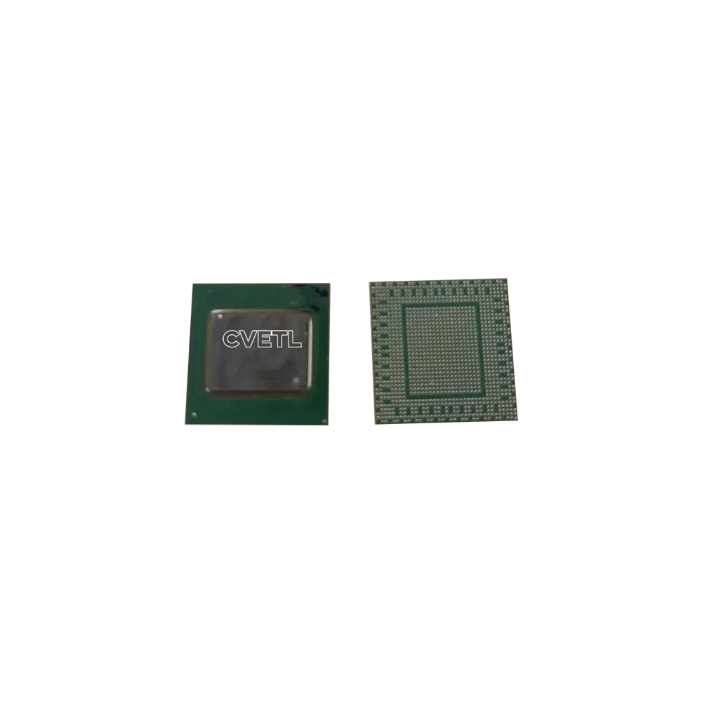
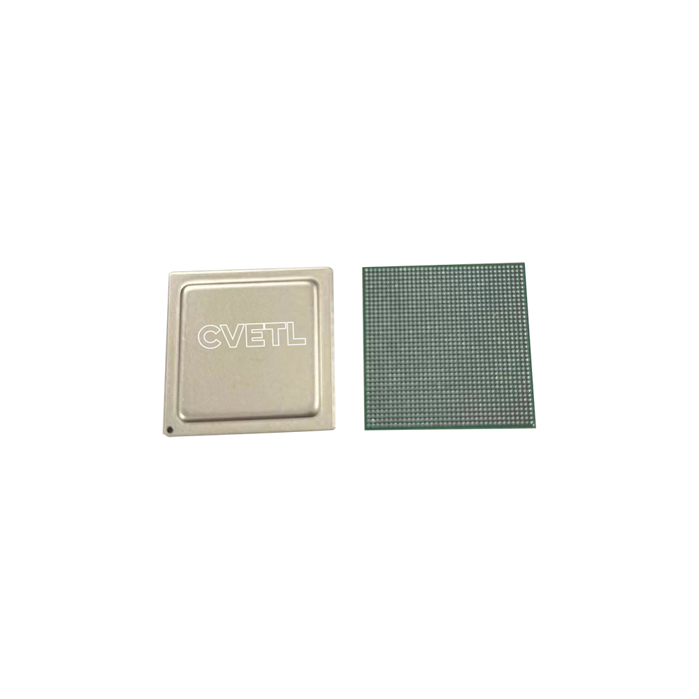
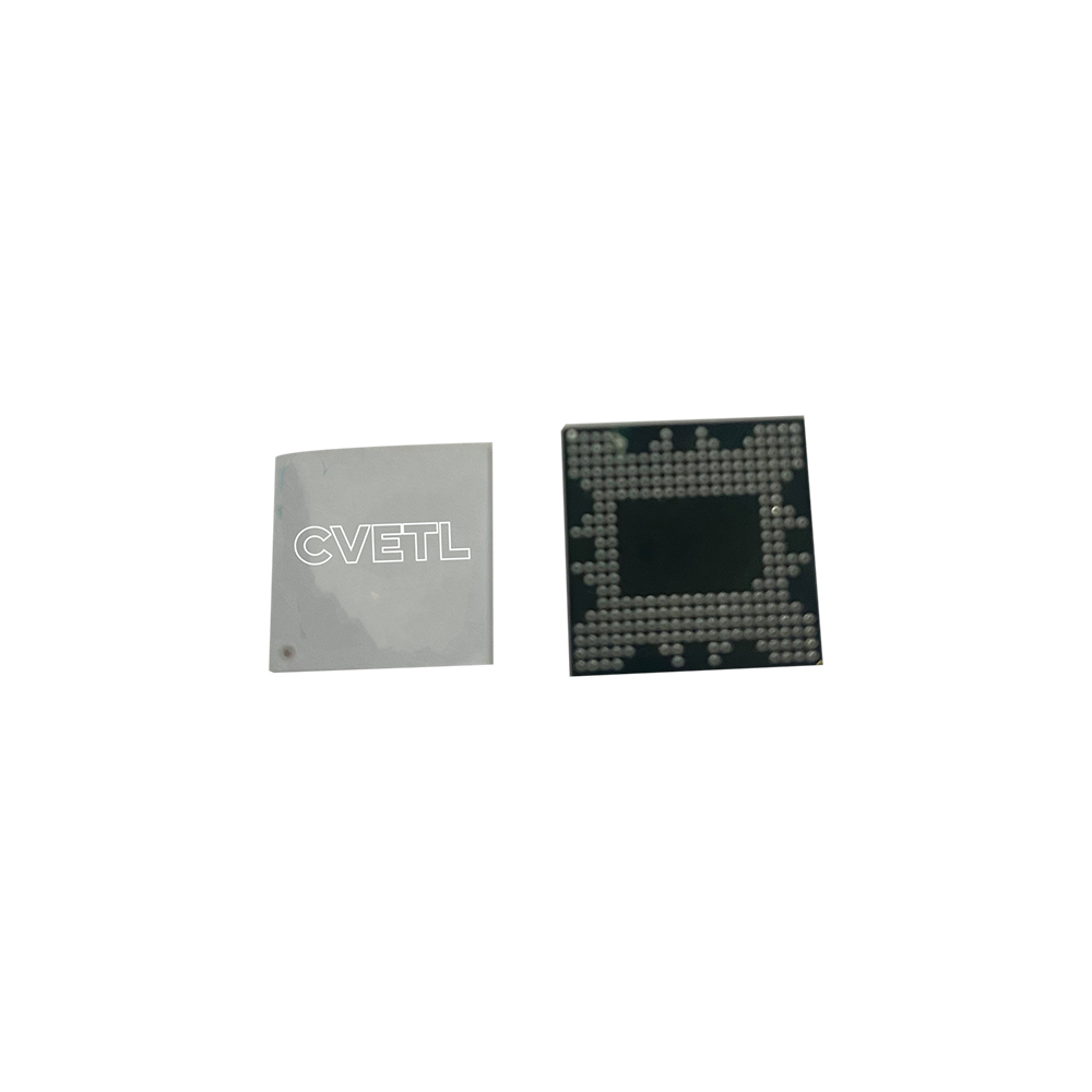
FCCSP
Cvetl is now offering Flip Chip CSP package; a flip chip solution for CSP packaging. Utilizing the eutectic solder bump flip chip interconnection technology, a peripheral or array flip chip bump design provides the shortest interconnection path as a replacement for conventional wire bonding. Based on the configuration of Siliconware's Thin and Fine-pitch BGA (TFBGA), the Flip Chip CSP package provides an easy-to-use construction for customers. Utilizing the fine line/space, state-of-the-art ultra fine mechanical drilled thin core laminate substrate, Siliconware's Flip Chip CSP is offering a costeffective option for high electrical performance CSP solution. Optional exposed die design allows the minimum package thickness down to 1.0 mm for handheld/portable electronics.
FEATURES
• 2-4 layers thin organic substrate
• Overmolded for excellent handling and reliability
• Minimum 125 µm bump pitch (peripheral array)
• Package sizes from 6x8 mm to 15x15 mm
• Minimum package thickness 1.0 mm (without overmolding), 1.2 mm for overmolded
• BGA ball pitch applicable on 0.5 ~ 1.0 mm